Co-reporter:Xuelu Hu, Hong Zhou, Zhenyu Jiang, Xiao Wang, Shuangping Yuan, Jianyue Lan, Yongping Fu, Xuehong Zhang, Weihao Zheng, Xiaoxia Wang, Xiaoli Zhu, Lei Liao, Gengzhao Xu, Song Jin, and Anlian Pan
ACS Nano October 24, 2017 Volume 11(Issue 10) pp:9869-9869
Publication Date(Web):September 18, 2017
DOI:10.1021/acsnano.7b03660
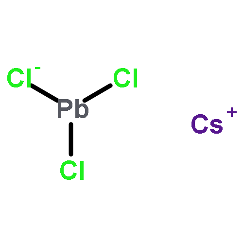
Metal halide perovskite nanostructures hold great promises as nanoscale light sources for integrated photonics due to their excellent optoelectronic properties. However, it remains a great challenge to fabricate halide perovskite nanodevices using traditional lithographic methods because the halide perovskites can be dissolved in polar solvents that are required in the traditional device fabrication process. Herein, we report single CsPbBr3 nanoplate electroluminescence (EL) devices fabricated by directly growing CsPbBr3 nanoplates on prepatterned indium tin oxide (ITO) electrodes via a vapor-phase deposition. Bright EL occurs in the region near the negatively biased contact, with a turn-on voltage of ∼3 V, a narrow full width at half-maximum of 22 nm, and an external quantum efficiency of ∼0.2%. Moreover, through scanning photocurrent microscopy and surface electrostatic potential measurements, we found that the formation of ITO/p-type CsPbBr3 Schottky barriers with highly efficient carrier injection is essential in realizing the EL. The formation of the ITO/p-type CsPbBr3 Schottky diode is also confirmed by the corresponding transistor characteristics. The achievement of EL nanodevices enabled by directly grown perovskite nanostructures could find applications in on-chip integrated photonics circuits and systems.Keywords: CsPbBr3 nanoplates; electroluminescence; lead halide perovskites; vapor growth;
Co-reporter:Hong Zhou, Shuangping Yuan, Xiaoxia Wang, Tao Xu, Xiao Wang, Honglai Li, Weihao Zheng, Peng Fan, Yunyun Li, Litao Sun, and Anlian Pan
ACS Nano 2017 Volume 11(Issue 2) pp:
Publication Date(Web):December 30, 2016
DOI:10.1021/acsnano.6b07374
Although great efforts have been devoted to the synthesis of halide perovskites nanostructures, vapor growth of high-quality one-dimensional cesium lead halide nanostructures for tunable nanoscale lasers is still a challenge. Here, we report the growth of high-quality all-inorganic cesium lead halide alloy perovskite micro/nanorods with complete composition tuning by vapor-phase deposition. The as-grown micro/nanorods are single-crystalline with a triangular cross section and show strong photoluminescence which can be tuned from 415 to 673 nm by varying the halide composition. Furthermore, these single-crystalline perovskite micro/nanorods themselves function as effective Fabry–Perot cavities for nanoscale lasers. We have realized room-temperature tunable lasing of cesium lead halide perovskite with low lasing thresholds (∼14.1 μJ cm–2) and high Q factors (∼3500).Keywords: cesium lead halide perovskites; triangular micro/nanorods; tunable lasers; vapor-phase growth;
Co-reporter:Honglai Li, Xueping Wu, Hongjun Liu, Biyuan Zheng, Qinglin Zhang, Xiaoli Zhu, Zheng Wei, Xiujuan Zhuang, Hong Zhou, Wenxin Tang, Xiangfeng DuanAnlian Pan
ACS Nano 2017 Volume 11(Issue 1) pp:
Publication Date(Web):December 19, 2016
DOI:10.1021/acsnano.6b07580
Composition-controlled growth of two-dimensional layered semiconductor heterostructures is crucially important for their applications in multifunctional integrated photonics and optoelectronics devices. Here, we report the realization of composition completely modulated layered semiconductor MoS2–MoS2(1–x)Se2x (0 < x < 1) lateral heterostructures via the controlled layer-selected atomic substitution of pregrown stacking MoS2, with a bilayer located at the center of a monolayer. Through controlling the reaction time, S at the monolayer MoS2 at the peripheral area can be selectively substituted by Se atoms at different levels, while the bilayer region at the center retains the original composition. Microstructure characterizations demonstrated the formation of lateral heterostructures with a sharp interface, with the composition at the monolayer area gradually modulated from MoS2 to MoSe2 and having high-quality crystallization at both the monolayer and the bilayer areas. Photoluminescence and Raman mapping studies exhibit the tunable optical properties only at the monolayer region of the as-grown heterostructures, which further demonstrates the realization of high-quality composition/bandgap modulated lateral heterostructures. This work offers an interesting and easy route for the development of high-quality layered semiconductor heterostructures for potential broad applications in integrated nanoelectronic and optoelectronic devices.Keywords: atomic substitution; lateral heterostructures; layered semiconductor; transition-metal dichalcogenides; tunable compositions;
Co-reporter:Xuehong Zhang;Shuzhen Yang;Hong Zhou;Junwu Liang;Huawei Liu;Hui Xia;Xiaoli Zhu;Ying Jiang;Qinglin Zhang;Wei Hu;Xiujuan Zhuang;Hongjun Liu;Weida Hu;Xiao Wang
Advanced Materials 2017 Volume 29(Issue 21) pp:
Publication Date(Web):2017/06/01
DOI:10.1002/adma.201604431
Methylammonium lead halide perovskites have attracted enormous attentions due to their superior optical and electronic properties. However, the photodetection at near-infrared telecommunication wavelengths is hardly achievable because of their wide bandgaps. Here, this study demonstrates, for the first time, novel perovskite–erbium silicate nanosheet hybrid photodetectors with remarkable spectral response at ≈1.54 µm. Under the near-infrared light illumination, the erbium silicate nanosheets can give strong upconversion luminescence, which will be well confined in their cavities and then be efficiently coupled into and simultaneously excite the adjacent perovskite to realize photodetection. These devices own prominent responsivity and external quantum efficiency as high as previously reported microscale silicon-based subbandgap photodetectors. More importantly, the photoresponse speed (≈900 µs) is faster by five orders than the ever reported hot electron silicon-based photodetectors at telecommunication wavelengths. The realization of perovskite-based telecommunication band photodetectors will open new chances for applications in advanced integrated photonics devices and systems.
Co-reporter:Xueping Wu;Honglai Li;Hongjun Liu;Xiujuan Zhuang;Xiao Wang;Xiaopeng Fan;Xidong Duan;Xiaoli Zhu;Qinglin Zhang;Alfred J. Meixner;Xiangfeng Duan
Nanoscale (2009-Present) 2017 vol. 9(Issue 14) pp:4707-4712
Publication Date(Web):2017/04/06
DOI:10.1039/C7NR00272F
Controllable synthesis of two-dimensional (2D) transition-metal dichalcogenides (TMDs) with tunable bandgaps is vital for their applications in nanophotonics, due to its efficient modulation of the physical and chemical properties of these atomic layered nanostructures. Here we report for the first time, the controllable synthesis of spatially composition-modulated WS2xSe2(1−x) nanosheets and WS2–WS2xSe2(1−x) lateral heterostructures by a developed one-step chemical vapor deposition (CVD) approach, as well as the understanding of their growth mechanism. During the growth, the composition was optically tuned along the plane of the atomic layered nanosheets through the precise control of evaporation sources. Microstructure characterization confirms the chemical identity of the composition modulated nanosheets, with S and Se contents gradually converting from the center to the edge. Local photoluminescence (PL) and Raman studies further demonstrate the position-dependent optical properties of the as-grown nanosheets, with the PL peak and Raman modes shifting in a wide range along the whole plane of the nanostructures, which are consistent with their tunable compositions and bandgaps. This demonstration of composition-modulated nanostructures provides a beneficial approach for the preparation of 2D semiconductor heterostructures and may open up a wide range of applications in nanoelectronics and optoelectronics.
Co-reporter:Xiaopeng Fan;Weihao Zheng;Hongjun Liu;Xiujuan Zhuang;Peng Fan;Yanfang Gong;Honglai Li;Xueping Wu;Ying Jiang;Xiaoli Zhu;Qinglin Zhang;Hong Zhou;Wei Hu;Xiao Wang;Xiangfeng Duan
Nanoscale (2009-Present) 2017 vol. 9(Issue 21) pp:7235-7241
Publication Date(Web):2017/06/01
DOI:10.1039/C7NR01345K
Recombination dynamics during photoluminescence (PL) in two-dimensional (2D) semiconducting transition metal dichalcogenides (TMDs) are complicated and can be easily affected by the surroundings because of their atomically thin structures. Herein, we studied the excitation power and temperature dependence of the recombination dynamics on the chemical vapor deposition-grown monolayer WS2via a combination of Raman, PL, and time-resolved PL spectroscopies. We found a red shift and parabolic intensity increase in the PL emission of the monolayer WS2 with the increasing excitation power and the decay time constants corresponding to the recombination of trions and excitons from transient PL dynamics. We attributed the abovementioned nonlinear changes in the PL peak positions and intensities to the combination of increasing carrier interaction and band structure renormalization rather than to the thermal effect from a laser. Furthermore, the excitation power-dependent Raman measurements support our conclusion. These findings and understanding will provide important information for the development of TMD-based optoelectronics and photonics.
Co-reporter:Huang Tan;Chao Fan;Liang Ma;Xuehong Zhang;Peng Fan;Yankun Yang
Nano-Micro Letters 2016 Volume 8( Issue 1) pp:29-35
Publication Date(Web):2016 January
DOI:10.1007/s40820-015-0058-0
InGaAs is an important bandgap-variable ternary semiconductor which has wide applications in electronics and optoelectronics. In this work, single-crystal InGaAs nanowires were synthesized by a chemical vapor deposition method. Photoluminescence measurements indicate the InGaAs nanowires have strong light emission in near-infrared region. For the first time, photodetector based on as-grown InGaAs nanowires was also constructed. It shows good light response over a broad spectral range in infrared region with responsivity of 6.5 × 10³ A W−1 and external quantum efficiency of 5.04 × 10⁵ %. This photodetector may have potential applications in integrated optoelectronic devices and systems.
Co-reporter:Xiujuan Zhuang;Pengfei Guo;Qinglin Zhang;Huawei Liu;Dan Li;Wei Hu
Nano Research 2016 Volume 9( Issue 4) pp:933-941
Publication Date(Web):2016 April
DOI:10.1007/s12274-015-0977-6
Low-dimensional semiconductor nanostructures have attracted much interest for applications in integrated photonic and optoelectronic devices. Band gap engineering within single semiconductor nanoribbons helps to manipulate photon behavior in two different cavities (in the width and length directions) and realize new photonic phenomena and applications. In this work, lateral composition-graded semiconductor nanoribbons were grown for the first time through an improved source-moving vapor phase route. Along the width of the nanoribbon, the material can be gradually tuned from pure CdS to a highly Se-doped CdSSe alloy with a corresponding band gap modulation from 2.42 to 1.94 eV. The achieved alloy ribbons are overall high-quality crystals, and the position-dependent band-edge photoluminescence (PL) emission had a peak wavelength continuously tuned from ~515 to ~640 nm. These ribbons can realize multi-color lasing with three groups of lasing modes centered at 519, 557, and 623 nm. It was confirmed that the red lasing was from optical resonance along the length direction, while the green and yellow lasing was from optical resonance along the width direction. These novel nanoribbon structures may be applied to many integrated photonic and optoelectronic devices.
Co-reporter:Pengfei Guo, Jinyou Xu, Ke Gong, Xia Shen, Yang Lu, Yang Qiu, Junqi Xu, Zhijun Zou, Chunlei Wang, Hailong Yan, Yongsong Luo, Anlian Pan, Han Zhang, Johnny C. Ho, and Kin Man Yu
ACS Nano 2016 Volume 10(Issue 9) pp:8474
Publication Date(Web):July 15, 2016
DOI:10.1021/acsnano.6b03458
We report the growth of high-quality CdS/CdSxSe1–x axial heterostructure nanowires (NWHs) via a temperature-controlled chemical vapor deposition method. Microstructural characterizations revealed that these NWHs have a single-crystalline structure with abrupt heterojunctions. Local photoluminescence and mapping near the heterojunctions show only two separated narrow band-edge emission bands from the two different adjacent semiconductors, further demonstrating the high-quality of these heterostructures. Moreover, the photodetector based on the single NWH shows a performance (higher responsivity (1.18 × 10² A/W), faster response speed (rise ∼68 μs, decay ∼137 μs), higher Ion/Ioff ratio (105), higher EQE (3.1 × 10⁴ %), and broader detection range (350–650 nm)) at room temperature superior to that of photodetectors based on single band gap nanostructures. This work suggests a much simpler route to achieve superior NWHs for applications in optoelectronic devices.Keywords: heterostructure; high performance; nanowire; photodetectors
Co-reporter:Honglai Li; Qinglin Zhang; Xidong Duan; Xueping Wu; Xiaopeng Fan; Xiaoli Zhu; Xiujuan Zhuang; Wei Hu; Hong Zhou; Anlian Pan;Xiangfeng Duan
Journal of the American Chemical Society 2015 Volume 137(Issue 16) pp:5284-5287
Publication Date(Web):April 14, 2015
DOI:10.1021/jacs.5b01594
Band gap engineering of transition-metal dichalcogenides is an important task for their applications in photonics, optoelectronics, and nanoelectronics. We report for the first time the continuous lateral growth of composition graded bilayer MoS2(1–x)Se2x alloys along single triangular nanosheets by an improved chemical vapor deposition approach. From the center to the edge of the nanosheet, the composition can be gradually tuned from x = 0 (pure MoS2) to x = 0.68, leading to the corresponding bandgap being continuously modulated from 1.82 eV (680 nm) to 1.64 eV (755 nm). Local photoluminescence scanning from the center to the edge gives single band edge emission peaks, indicating high crystalline quality for the achieved alloy nanosheets, which was further demonstrated by the microstructure characterizations. These novel 2D structures offer an interesting system for probing the physical properties of layered materials and exploring new applications in functional nanoelectronic and optoelectronic devices.
Co-reporter:Yunyun Li, Junwu Liang, Qinglin Zhang, Zidong Zhou, Honglai Li, Xiaopeng Fan, Xiaoxia Wang, Peng Fan, Yankun Yang, Pengfei Guo, Xiujuan Zhuang, Xiaoli Zhu, Lei Liao, Anlian Pan
Optics Communications 2015 Volume 354() pp:168-173
Publication Date(Web):1 November 2015
DOI:10.1016/j.optcom.2015.05.058
•A hybrid metal–dielectric–semiconductor nanostructure correlating the metal nanodisks and semiconductor nanoribbon is proposed.•The nanostructure is fabricated through CVD and EBL technique.•The measurement is realized by combing AFM with the defocused imaging technique which is realized in a normal wide-field fluorescence microscope.•The beam splitting mechanism of this nanostructure is investigated by numerical simulation.•The beam splitting mechanism reveals that this hybrid metal–dielectric–semiconductor nanostructure can be applied as optical waveguide beam splitter.Miniature integration is desirable for the future photonics circuit. Low-dimensional semiconductor and metal nanostructures is the potential building blocks in compact photonic circuits for their unique electronic and optical properties. In this work, a hybrid metal–dielectric–semiconductor nanostructure is designed and fabricated to realizing a nano-scale optical waveguide beam splitter, which is constructed with the sandwiched structure of a single CdS nanoribbon/HfO2 thin film/Au nanodisk arrays. Micro-optical investigations reveal that the guided light outputting at the terminal end of the CdS ribbon is well separated into several light spots. Numerical simulations further demonstrate that the beam splitting mechanism is attributed to the strong electromagnetic coupling between the Au nanodisks and light guided in the nanoribbon. The number of the split beams (light spots) at the terminal end of the nanoribbon is mainly determined by the number of the Au nanodisk rows, as well as the distance of the blank region between the nanodisks array and the end of the CdS ribbon, owing to the interference between the split beams. These optical beam splitters may find potential applications in high-density integrated photonic circuits and systems.
Co-reporter:Chao Fan;Qinglin Zhang;Xiaoli Zhu;Xiujuan Zhuang
Science Bulletin 2015 Volume 60( Issue 19) pp:1674-1679
Publication Date(Web):2015 October
DOI:10.1007/s11434-015-0900-2
ZnSe nanoribbons were synthesized with chemical vapor deposition route. The excitation power-dependent photoluminescence and surface photovoltage (SPV) techniques were used to study the optoelectronic properties of the as-grown ZnSe nanoribbons. Three deep defect (DD)-related emission bands, respectively, centered at 623 nm (DD1), 563 nm (DD2) and 525 nm (DD3), emerge orderly with increasing the excitation power, which is attributed to the saturation of the DD states from deeper to shallower level. The SPV spectrum and the corresponding phase spectrum show that DD1 mainly acts as recombination center, while DD2 and DD3 can act as both the recombination center and electron traps. The influence of the trapping electrons on the SPV response dynamic was studied with transient SPV.ZnSe因其2.7 eV的禁带宽度,在蓝光发射器件领域具有潜在的应用前景,也使得ZnSe纳米结构近年来倍受关注。但是,ZnSe晶体结构中存在大量隙间缺陷态,会导致弱的蓝光发射带,同时也阻碍了ZnSe的实际应用。清晰的理解与缺陷态相关的光生电荷行为,如:复合、分离等,对实现基于ZnSe纳米结构的高性能光电器件具有重要意义。本文结合激发光强依赖的荧光光谱(PL)和表面光电压技术对ZnSe纳米带的各个缺陷能级在光生电荷的复合和分离过程中起的作用进行了研究。激发光强依赖的PL研究结果发现,ZnSe纳米带具有3个隙间态能级(DD),随激发光强由弱到强,中心波长在623 nm (DD1), 563 nm (DD2)和525 nm (DD3)的发射带依次出现。光电压谱研究结果表明,只有较浅的2个能级DD2和DD3与基态间的跃迁可以实现光生电荷的分离,产生光伏响应。瞬态光伏研究结果表明,缺陷态对光生电荷的俘获延长了光生电荷的寿命,减缓了光伏响应的衰减。
Co-reporter:Pinyun Ren;Wei Hu;Qinglin Zhang;Xiaoli Zhu;Xiujuan Zhuang;Liang Ma;Xiaopeng Fan;Hong Zhou;Lei Liao;Xiangfeng Duan
Advanced Materials 2014 Volume 26( Issue 44) pp:7444-7449
Publication Date(Web):
DOI:10.1002/adma.201402945
Co-reporter:Pengfei Guo;Wei Hu;Qinglin Zhang;Xiujuan Zhuang;Xiaoli Zhu;Hong Zhou;Zhengping Shan;Jinyou Xu
Advanced Materials 2014 Volume 26( Issue 18) pp:2844-2849
Publication Date(Web):
DOI:10.1002/adma.201304967
Co-reporter:Liang Ma, Wei Hu, Qinglin Zhang, Pinyun Ren, Xiujuan Zhuang, Hong Zhou, Jinyou Xu, Honglai Li, Zhengping Shan, Xiaoxia Wang, Lei Liao, H. Q. Xu, and Anlian Pan
Nano Letters 2014 Volume 14(Issue 2) pp:694-698
Publication Date(Web):January 1, 2014
DOI:10.1021/nl403951f
Nanoscale near-infrared photodetectors are attractive for their potential applications in integrated optoelectronic devices. Here we report the synthesis of GaSb/GaInSb p–n heterojunction semiconductor nanowires for the first time through a controllable chemical vapor deposition (CVD) route. Based on these nanowires, room-temperature, high-performance, near-infrared photodetectors were constructed. The fabricated devices show excellent light response in the infrared optical communication region (1.55 μm), with an external quantum efficiency of 104, a responsivity of 103 A/W, and a short response time of 2 ms, which shows promising potential applications in integrated photonics and optoelectronics devices or systems.
Co-reporter:Yaqin Zou, Honglai Li, Pinyun Ren, Jinyou Xu, Liang Ma, Xiaoxia Wang, Xiaopeng Fan, Zhengping Shan, Xiujuan Zhuang, Hong Zhou, Xiaoli Zhu, Qinglin Zhang, Anlian Pan
Materials Letters 2014 Volume 129() pp:118-121
Publication Date(Web):15 August 2014
DOI:10.1016/j.matlet.2014.05.015
•ZnSe nanoribbons were fabricated by a chemical vapor deposition (CVD) route.•Spatially resolved photoluminescence is studied in the μ-PL spectra and mappings.•The DD related emission is researched to be attributed to the structure defects mainly located at the edges.•The temperature dependent PL spectra demonstrate the carriers׳ transfer among the different defect states.ZnSe nanoribbons were synthesized and characterized with microphotoluminescence (μ-PL) spectra and mappings. The μ-PL results show that the near band edge (BE) and the deep defect (DD) level related emissions are predominantly located at the central and the edge region of the ribbons, respectively. Combining with the HRTEM, the DD related emission is attributed to the structure defects mainly located at the edge of the ribbon. It is found that the DD related emission consists of three bands, centered at 635, 560 and 535 nm, respectively. The temperature dependent PL spectra further demonstrate that the carriers transfer among the different defect states through the thermally activated mechanism. The results provide more direct evidence about the origin of trap state related emissions in ZnSe nanostructures.
Co-reporter:Zidong Zhou, Pengbin He, Jinyou Xu, Xiujuan Zhuang, Yunyun Li, Anlian Pan
Optics Communications 2014 Volume 312() pp:280-283
Publication Date(Web):1 February 2014
DOI:10.1016/j.optcom.2013.09.041
•We propose and investigate a compact gradient index plasmonic ring resonator (Grin PRR).•The extinction ratio of Grin PRR can be optimized by varying the index gradient for any radius.•Grin PRR has both high extinction ratio and smaller size footprint.We propose and investigate a compact gradient index plasmonic ring resonator (Grin PRR) with strong light confinement and extinction ratio based on finite element method (FEM). Theoretical simulation reveals that the change of index gradient influences the resonant frequency, Q factor and the mode volume. Significantly, it is demonstrated that the extinction ratio of Grin PRR can be optimized by varying the index gradient for any radius. Index gradient can enhance extinction ratio at settled size, so this structure has both high extinction ratio and smaller size footprint. It could be very promising for the high-density optical integration.
Co-reporter:Pinyun Ren;Xiaoli Zhu;Jinyun Han;Jinyou Xu;Liang Ma;Honglai Li
Nano-Micro Letters 2014 Volume 6( Issue 4) pp:301-306
Publication Date(Web):2014 October
DOI:10.1007/s40820-014-0002-8
In this work, we synthesized high-quality InAs nanowires by a convenient chemical vapor deposition method, and developed a simple laser heating method to measure the thermal conductivity of a single InAs nanowire in air. During the measurement, a focused laser was used to heat one end of a freely suspended nanowire, with its other end embedded into a carbon conductive adhesive. In order to obtain the thermal conductivity of InAs nanowires, the heat loss in the heat transfer process was estimated, which includes the heat loss through air conduction, the heat convection, and the radiation loss. The absorption ratio of the laser power in the InAs nanowire was calculated. The result shows that the thermal conductivity of InAs nanowires monotonically increases from 6.4 W m−1 K−1 to 10.5 W m−1 K−1 with diameters increasing from 100 nm to 190 nm, which is ascribed to the enhanced phonon-boundary scattering.
Co-reporter:Pengfei Guo, Xiujuan Zhuang, Jinyou Xu, Qinglin Zhang, Wei Hu, Xiaoli Zhu, Xiaoxia Wang, Qiang Wan, Pengbin He, Hong Zhou, and Anlian Pan
Nano Letters 2013 Volume 13(Issue 3) pp:1251-1256
Publication Date(Web):February 19, 2013
DOI:10.1021/nl3047893
Low-threshold nanoscale lasers are attractive for their promising applications in highly integrated photonic devices and systems. Here we report the controllable growth of composition-symmetric CdSxSe1–x nanowires by using a multistep thermal evaporation route with moving sources. Microstructure analyses reveal the obtained wires are high-quality single crystals with the composition gradually changed from the center toward their both ends. Under laser illumination, these wires exhibit symmetrical color distribution along the length direction, with red at the center and green at the both ends. Optically pumped lasing is realized at room temperature using these composition-symmetric nanowires, with the threshold several times lower than that of composition-homogeneous wires. This new nanowire structure will have potential applications as low-threshold nanoscale lasers in integrated nanophotonics.
Co-reporter:Jinyou Xu, Xiujuan Zhuang, Pengfei Guo, Qinglin Zhang, Liang Ma, Xiaoxia Wang, Xiaoli Zhu and Anlian Pan
Journal of Materials Chemistry A 2013 vol. 1(Issue 28) pp:4391-4396
Publication Date(Web):14 May 2013
DOI:10.1039/C3TC30492B
High-quality dilute tin-doped CdS nanowires with tunable trap-state emissions were grown via simple thermal evaporation with a moving source for studying the influence of trap states on optical waveguiding. Our results demonstrate that the guiding efficiency of these wires is significantly enhanced compared to that of the pure CdS wires. Theoretical simulation based on the fundamental optical absorption principle of semiconductors further reveals that this trap-state enhanced optical waveguiding is attributed to the passive guiding process of the trap-state emissions along these wires. To the best of our knowledge, this study is the first demonstration of using dopants to shift emission away from bandgap absorption for the purpose of optical waveguiding enhancement, which is significant for understanding and optimizing the optical transport ability of semiconductor nanostructures.
Co-reporter:Pengfei Guo, Jinyou Xu, Xiujuan Zhuang, Wei Hu, Xiaoli Zhu, Hong Zhou, Lijuan Tang and Anlian Pan
Journal of Materials Chemistry A 2013 vol. 1(Issue 3) pp:566-571
Publication Date(Web):30 Oct 2012
DOI:10.1039/C2TC00088A
Inspired by the good match between the surface-plasmon energy of Au nanoparticles and the emitted photon energy of CdS nanowires, CdS–SiO2 core–shell nanowires with Au nanoparticles attached (CdS–SiO2–Au) were prepared to investigate the interaction between the semiconductor and the metal. Photoluminescent and lifetime measurement reveal that the band-edge emission of CdS nanowires in this hybrid structure has a fivefold enhancement compared with pure CdS nanowires due to the surface plasmon resonance. In addition, the existence of an optimized thickness of the SiO2 layer for the emission enhancement indicates that the interactions between the metal and the semiconductor occur constructively only at appropriate distances. These CdS–SiO2–Au nanowires with tailored morphologies and enhanced band-edge emission have potential applications in solar cells, photodetectors and bio-nanotechnology.
Co-reporter:Yicheng Wang, Jinyou Xu, Pinyun Ren, Qinglin Zhang, Xiujuan Zhuang, Xiaoli Zhu, Qiang Wan, Hong Zhou, Wei Hu and Anlian Pan
Physical Chemistry Chemical Physics 2013 vol. 15(Issue 8) pp:2912-2916
Publication Date(Web):22 Jan 2013
DOI:10.1039/C2CP43718J
Composition-tunable semiconductor alloy nanowires are emerging as an important class of materials for the realization of high-performance laterally-arranged multiple bandgap (LAMB) solar cells. Here we report the first growth of GaZnSeAs quaternary alloy nanowires with composed elements between two different groups using a temperature/space-selective CVD route. Under laser excitation, these special quaternary alloy nanowires exhibit composition-related characteristic emissions, with peak wavelengths gradually tunable from 470 nm (2.64 eV) to 832 nm (1.49 eV), covering almost the entire visible spectrum. Surface photovoltage measurements further reveal that these alloy nanowires have tunable bandgaps along the length of the substrate, making them promising candidates for developing high-efficiency LAMB solar cells. These quaternary alloy nanowires represent a new advancement in material synthesis and would have potential applications in a variety of function-tunable and broadband-response optoelectronic devices.
Co-reporter:Yicheng Wang, Jinyou Xu, Pinyun Ren, Xiujuan Zhuang, Hong Zhou, Qinglin Zhang, Xiaoli Zhu, Anlian Pan
Materials Letters 2013 Volume 105() pp:90-94
Publication Date(Web):15 August 2013
DOI:10.1016/j.matlet.2013.04.054
•Completely composition-tunable Cd1−xZnxTe alloy nanostructures were synthesized.•These Cd1−xZnxTe alloy nanostructures exhibit composition-related tunable bandgaps.•The varied bandgaps from 2.24 eV to 1.51 eV are integrated on a single substrate.•These alloy nanostructures would be used in function-tunable optoelectronic devices.Semiconductor alloy nanostructures with tunable compositions provide excellent material platforms for function-tunable and/or broadband-response optoelectronic applications. Here we report the growth of high quality single-crystalline Cd1-xZnxTe alloy nanostructures in the full-composition region on a single substrate via a simple co-thermal evaporation route. X-ray diffraction (XRD) and transmission electron microscopy (TEM) characterizations confirm that the lattice parameters gradually increase with the increase of cadmium contents. Photoluminescence (PL) measurements show that these composition-tunable alloy nanostructures exhibit near-bandedge emissions, with peaks wavelength continuously changing from 554 nm to 819 nm. These alloy nanostructures will find potential applications in near-infrared function-tunable optoelectronic devices, such as high-performance laterally-arranged multiple-bandgap solar cells, variable-wavelength photodetectors and so on.
Co-reporter:Jiajie Guo, Jinyou Xu, Xiujuan Zhuang, Yicheng Wang, Hong Zhou, Zhengping Shan, Pinyun Ren, Pengfei Guo, Qinglin Zhang, Qiang Wan, Xiaoli Zhu, Anlian Pan
Chemical Physics Letters 2013 Volume 576() pp:26-30
Publication Date(Web):28 June 2013
DOI:10.1016/j.cplett.2013.05.013
Highlights
- •
The relationship between microstructure and photoluminescence for ZnTe nanostructures was firstly investigated.
- •
The emission bands redshift with increasing the excitation intensity.
- •
The redshift magnitude is highly related to the structures.
Co-reporter:Quanming Hao, Jingyou Xu, Xiujuan Zhuang, Qinglin Zhang, Qiang Wan, Huayong Pan, Xiaoli Zhu, Anlian Pan
Materials Letters 2013 100() pp: 141-144
Publication Date(Web):
DOI:10.1016/j.matlet.2013.02.091
Co-reporter:Xiujuan Zhuang;C. Z. Ning
Advanced Materials 2012 Volume 24( Issue 1) pp:13-33
Publication Date(Web):
DOI:10.1002/adma.201103191
Abstract
Semiconductor alloy nanowires with spatially graded compositions (and bandgaps) provide a new material platform for many new multifunctional optoelectronic devices, such as broadly tunable lasers, multispectral photodetectors, broad-band light emitting diodes (LEDs) and high-efficiency solar cells. In this review, we will summarize the recent progress on composition graded semiconductor alloy nanowires with bandgaps graded in a wide range. Depending on different growth methods and material systems, two typical nanowire composition grading approaches will be presented in detail, including composition graded alloy nanowires along a single substrate and those along single nanowires. Furthermore, selected examples of applications of these composition graded semiconductor nanowires will be presented and discussed, including tunable nanolasers, multi-terminal on-nanowire photodetectors, full-spectrum solar cells, and white-light LEDs. Finally, we will make some concluding remarks with future perspectives including opportunities and challenges in this research area.
Co-reporter:Jinyou Xu, Xiujuan Zhuang, Pengfei Guo, Qinglin Zhang, Weiqing Huang, Qiang Wan, Wei Hu, Xiaoxia Wang, Xiaoli Zhu, Changzeng Fan, Zongyin Yang, Limin Tong, Xiangfeng Duan, and Anlian Pan
Nano Letters 2012 Volume 12(Issue 9) pp:5003-5007
Publication Date(Web):August 3, 2012
DOI:10.1021/nl302693c
Compact wavelength-sensitive optical components are desirable for optical information processing and communication in photonic integrated system. In this work, optical waveguiding along single composition-graded CdSxSe1-x nanowires were systematically investigated. Under a focused laser excitation, the excited light can be guided passively along the bandgap-increased direction of the nanowire, keeping the photonic energy of the guided light almost unchanged during the whole propagation. In comparison, the excited light is guided actively through incessantly repeated band-to-band reabsorption and re-emitting processes along the bandgap-decreased direction, resulting in a gradual wavelength conversion during propagation. On the basis of this wavelength-converted waveguiding, a concept of nanoscale wavelength splitter is demonstrated by assembling a graded nanowire with several composition-uniform nanowires into branched nanowire structure. Our study indicates that composition-graded semiconductor nanowires would open new exciting opportunities in developing new wavelength-sensitive optical components for integrated nanophotonic devices.
Co-reporter:Jinyou Xu, Hongxing Li, Xiujuan Zhuang, Qinglin Zhang, Pengfei Guo, Liang Ma and Anlian Pan
Nanoscale 2012 vol. 4(Issue 5) pp:1481-1485
Publication Date(Web):02 Nov 2011
DOI:10.1039/C1NR10844A
A new type of chain-like Si@SiSe2 nanowire heterostructures has been successfully synthesized via a one-step Au-catalyzed chemical vapor deposition (CVD) route. The composition and microstructure of the achieved structures were investigated by scanning electron microscope (SEM), energy dispersive X-ray spectroscopy (EDX), transmission electron microscope (TEM) and micro-Raman spectroscopy. Optical characterization was investigated using a confocal photoluminescent system with an Ar+ laser (488 nm) as the excitation source. The results reveal that these chain-like structures emit pronounced and broadband red light, even visible with the naked eye at room temperature. A self-organization model was proposed to illustrate the formation of these heterostructures, and the photoluminescent properties were discussed in detail. These new Si-based nanostructures may be helpful for further study of the basic physical properties of SiSe2 and will find interesting applications in nanophotonic technologies and devices.
Co-reporter:Zongyin Yang, Jinyou Xu, Pan Wang, Xiujuan Zhuang, Anlian Pan, and Limin Tong
Nano Letters 2011 Volume 11(Issue 11) pp:5085-5089
Publication Date(Web):October 19, 2011
DOI:10.1021/nl203529h
We demonstrated a substrate-moving vapor–liquid–solid (VLS) route for growing composition gradient ZnCdSSe alloy nanowires. Relying on temperature-selected composition deposition along their lengths, single tricolor ZnCdSSe alloy nanowires with engineerable band gap covering the entire visible range were obtained. The photometric property of these tricolor nanowires, which was determined by blue-, green-, and red-color emission intensities, can be in turn controlled by their corresponding emission lengths. More particularly, under carefully selected growth conditions, on-nanowire white light emission has been achieved. Band-gap-engineered semiconductor alloy nanowires demonstrated here may find applications in broad band light absorption and emission devices.
Co-reporter:Qinglin Zhang, Huawei Liu, Pengfei Guo, Dan Li, Peng Fan, Weihao Zheng, Xiaoli Zhu, Ying Jiang, Hong Zhou, Wei Hu, Xiujuan Zhuang, Hongjun Liu, Xiangfeng Duan, Anlian Pan
Nano Energy (February 2017) Volume 32() pp:
Publication Date(Web):February 2017
DOI:10.1016/j.nanoen.2016.12.014
•CdS-CdSSe-CdS axial nanowire heterostructures with highly crystallized and composition sharp interface are grown with a source switching vapor growth route.•Green (~516.4 nm) and red (~597.9 nm) color lasing are realized with the threshold of the red lower than that of the green one, which indicates the individual wires are good waveguide and resonant cavity.•Time-resolved photoluminescence characterizations reveal Energy transfer from the CdS to the CdSSe segments, corresponding to the interaction of the guided green light with CdSSe at the hetero-interfaces.Well understanding the interfacial carrier dynamics in semiconductor axial nanowire (NW) heterostructures is crucial important for the performance optimization of integrated photonics and optoelectronics devices. However, the growth of high-quality semiconductor axial NW heterostructures still remains a great challenge. Here, we develop a source switching vapor growth route and demonstrate the successful growth of CdS-CdSSe-CdS axial NW heterostructures with highly crystallized and composition sharp interface, which acts as the model material for the study of interfacial carrier dynamics. Under femtosecond laser pumping, the achieved NW heterostructures can simultaneously give lasing at the green (~516.4 nm) and red (~597.9 nm) spectral regions, demonstrating the well radial confinement of the both color emitted light. Time-resolved photoluminescence (PL) measurements reveal the energy transfer (ET) from the CdS to the CdSSe segments corresponds to the interaction of the guided green light with CdSSe at the hetero-interfaces, which makes the CdSSe segment have higher carrier density and emission efficiency, resulting in the more obvious power induced blueshift and lower lasing threshold comparing with the green emission. These obtained CdS-CdSSe-CdS axial NW heterostructures with effective ET have the potential applications in high performance optical and optoelectronic nanoscaled devices, like nanolaser, photodetectors, waveguide etc.We realize the controlled growth of CdS-CdSSe-CdS axial nanowire heterostructures with highly crystallized and composition sharp interface. Optically pumped dual-wavelength lasing is demonstrated at room temperature based on these unique nanowire heterostructures. Time-resolved PL measurements reveal the energy transfer from the CdS segment to the CdSSe segment, which plays important roles on the lasing activity of the heterostructures.
Co-reporter:Jinyou Xu ; Liang Ma ; Pengfei Guo ; Xiujuan Zhuang ; Xiaoli Zhu ; Wei Hu ; Xiangfeng Duan
Journal of the American Chemical Society () pp:
Publication Date(Web):July 17, 2012
DOI:10.1021/ja3050458
Nanoscale dual-wavelength lasers are attractive for their potential applications in highly integrated photonic devices. Here we report the growth of nanoribbon lateral heterostructures made of a CdSxSe1–x central region with epitaxial CdS lateral sides using a multistep thermal evaporation route with a moving source. Under laser excitation, the emission of these ribbons indicates sandwich-like structures along the width direction, with characteristic red emission in the center and green emission at both edges. More importantly, dual-wavelength lasing with tunable wavelengths is demonstrated at room temperature based on these single-nanoribbon heterostructures for the first time. These achievements represent a significant advance in designing nanoscale dual-wavelength lasers and have the potential to open up new and exciting opportunities for diverse applications in integrated photonics, optoelectronics, and sensing.
Co-reporter:Honglai Li ; Xidong Duan ; Xueping Wu ; Xiujuan Zhuang ; Hong Zhou ; Qinglin Zhang ; Xiaoli Zhu ; Wei Hu ; Pinyun Ren ; Pengfei Guo ; Liang Ma ; Xiaopeng Fan ; Xiaoxia Wang ; Jinyou Xu ; Anlian Pan ;Xiangfeng Duan
Journal of the American Chemical Society () pp:
Publication Date(Web):February 24, 2014
DOI:10.1021/ja500069b
Band gap engineering of atomically thin two-dimensional layered materials is critical for their applications in nanoelectronics, optoelectronics, and photonics. Here we report, for the first time, a simple one-step chemical vapor deposition approach for the simultaneous growth of alloy MoS2xSe2(1–x) triangular nanosheets with complete composition tunability. Both the Raman and the photoluminescence studies show tunable optical properties consistent with composition of the alloy nanosheets. Importantly, all samples show a single bandedge emission peak, with the spectral peak position shifting from 668 nm (for pure MoS2) to 795 nm (for pure MoSe2), indicating the high quality for these complete composition alloy nanosheets. These band gap engineered 2D structures could open up an exciting opportunity for probing their fundamental physical properties in 2D and may find diverse applications in functional electronic/optoelectronic devices.
Co-reporter:Yicheng Wang, Jinyou Xu, Pinyun Ren, Qinglin Zhang, Xiujuan Zhuang, Xiaoli Zhu, Qiang Wan, Hong Zhou, Wei Hu and Anlian Pan
Physical Chemistry Chemical Physics 2013 - vol. 15(Issue 8) pp:NaN2916-2916
Publication Date(Web):2013/01/22
DOI:10.1039/C2CP43718J
Composition-tunable semiconductor alloy nanowires are emerging as an important class of materials for the realization of high-performance laterally-arranged multiple bandgap (LAMB) solar cells. Here we report the first growth of GaZnSeAs quaternary alloy nanowires with composed elements between two different groups using a temperature/space-selective CVD route. Under laser excitation, these special quaternary alloy nanowires exhibit composition-related characteristic emissions, with peak wavelengths gradually tunable from 470 nm (2.64 eV) to 832 nm (1.49 eV), covering almost the entire visible spectrum. Surface photovoltage measurements further reveal that these alloy nanowires have tunable bandgaps along the length of the substrate, making them promising candidates for developing high-efficiency LAMB solar cells. These quaternary alloy nanowires represent a new advancement in material synthesis and would have potential applications in a variety of function-tunable and broadband-response optoelectronic devices.
Co-reporter:Pengfei Guo, Jinyou Xu, Xiujuan Zhuang, Wei Hu, Xiaoli Zhu, Hong Zhou, Lijuan Tang and Anlian Pan
Journal of Materials Chemistry A 2013 - vol. 1(Issue 3) pp:NaN571-571
Publication Date(Web):2012/10/30
DOI:10.1039/C2TC00088A
Inspired by the good match between the surface-plasmon energy of Au nanoparticles and the emitted photon energy of CdS nanowires, CdS–SiO2 core–shell nanowires with Au nanoparticles attached (CdS–SiO2–Au) were prepared to investigate the interaction between the semiconductor and the metal. Photoluminescent and lifetime measurement reveal that the band-edge emission of CdS nanowires in this hybrid structure has a fivefold enhancement compared with pure CdS nanowires due to the surface plasmon resonance. In addition, the existence of an optimized thickness of the SiO2 layer for the emission enhancement indicates that the interactions between the metal and the semiconductor occur constructively only at appropriate distances. These CdS–SiO2–Au nanowires with tailored morphologies and enhanced band-edge emission have potential applications in solar cells, photodetectors and bio-nanotechnology.
Co-reporter:Jinyou Xu, Xiujuan Zhuang, Pengfei Guo, Qinglin Zhang, Liang Ma, Xiaoxia Wang, Xiaoli Zhu and Anlian Pan
Journal of Materials Chemistry A 2013 - vol. 1(Issue 28) pp:NaN4396-4396
Publication Date(Web):2013/05/14
DOI:10.1039/C3TC30492B
High-quality dilute tin-doped CdS nanowires with tunable trap-state emissions were grown via simple thermal evaporation with a moving source for studying the influence of trap states on optical waveguiding. Our results demonstrate that the guiding efficiency of these wires is significantly enhanced compared to that of the pure CdS wires. Theoretical simulation based on the fundamental optical absorption principle of semiconductors further reveals that this trap-state enhanced optical waveguiding is attributed to the passive guiding process of the trap-state emissions along these wires. To the best of our knowledge, this study is the first demonstration of using dopants to shift emission away from bandgap absorption for the purpose of optical waveguiding enhancement, which is significant for understanding and optimizing the optical transport ability of semiconductor nanostructures.