Co-reporter:Jingjie Li, Xinhong Cheng, Qian Wang, Li Zheng, Lingyan Shen, Xinchang Li, Dongliang Zhang, Hongyue Zhu, DaShen Shen, Yuehui Yu
Materials Science in Semiconductor Processing 2017 Volume 67(Volume 67) pp:
Publication Date(Web):15 August 2017
DOI:10.1016/j.mssp.2017.05.022
In this work, we performed an inductively coupled plasma (ICP) etching of SiC substrates using different masks including SiO2, Ni, Ni/SiO2 and Ni/Al2O3, and the properties of trenches were systemically analyzed. In comparison with other three masks, Ni/Al2O3 mask prevented contamination of F or Ni element from diffusion into SiC, and achieved the optimized trench morphology with a surface roughness of 0.2 nm, steep sidewall and no micro-trench at the corner. Al2O3 dielectric films were deposited on trenches by plasma enhanced atomic layer deposition (PEALD), and its critical breakdown electrical field was much higher with Ni/Al2O3 mask, which could reach 7.7 MV/cm. So it was believed that Ni/Al2O3 mask ensured the formation of SiC trench with superior morphology.
Co-reporter:Qian Wang, Xinhong Cheng, Li Zheng, Peiyi Ye, Menglu Li, Lingyan Shen, Jingjie Li, Dongliang Zhang, Ziyue Gu, Yuehui Yu
Applied Surface Science 2017 Volume 410(Volume 410) pp:
Publication Date(Web):15 July 2017
DOI:10.1016/j.apsusc.2017.03.114
•The 4H-SiC MOS capacitor with an untra-thin LaSiOx passivation layer and Al2O3 gate dielectric was fabricated.•The detrimental SiOx interfacial layer could be effectively restrained by the LaSiOx passivation layer.•The passivation mechanism of LaSiOx was analyzed by HRTEM, XPS and electrical measurements.•The 4H-SiC MOS capacitor with a LaSiOx passivation layer shows excellent device characteristics.•This technique provides an efficient path to improve dielectrics/4H-SiC interfaces for future high-power device applications.The detrimental sub-oxide (SiOx) interfacial layer formed during the 4H-SiC metal-oxide-semiconductor (MOS) capacitor fabrication will drastically damage its device performance. In this work, an ultrathin lanthanum silicate (LaSiOx) passivation layer was introduced to enhance the interfacial and electrical characteristics of 4H-SiC MOS capacitor with Al2O3 gate dielectric. The interfacial LaSiOx formation was investigated by high resolution transmission electron microscopy and X-ray photoelectron spectroscopy. The 4H-SiC MOS capacitor with ultrathin LaSiOx passivation interlayer shows excellent interfacial and electrical characteristics, including lower leakage current density, higher dielectric breakdown electric field, smaller C–V hysteresis, and lower interface states density and border traps density. The involved mechanism implies that the LaSiOx passivation interlayer can effectively restrain SiOx formation and improve the Al2O3/4H-SiC interface quality. This technique provides an efficient path to improve dielectrics/4H-SiC interfaces for future high-power device applications.
Co-reporter:Qian Wang;Li Zheng;Lingyan Shen;Jingjie Li;Dongliang Zhang;Ru Qian;Yuehui Yu
RSC Advances (2011-Present) 2017 vol. 7(Issue 19) pp:11745-11751
Publication Date(Web):2017/02/13
DOI:10.1039/C6RA27190A
In this paper, AlNO nano-films have been deposited on an AlGaN/GaN heterojunction by alternating growth of AlN and Al2O3 using plasma enhanced atomic layer deposition (PEALD). With optimized AlN layer insertion in Al2O3, the oxygen is effectively blocked from diffusing to the AlGaN surface and the formation of detrimental Ga–O bonds is significantly suppressed. Owing to the negative fixed charges in Al2O3, provided by the incorporated nitrogen, the flat band voltage (Vfb) of the AlNO/AlGaN/GaN metal–insulator–semiconductor (MIS) diode exhibits a positive shift of 1.50 V, compared with the Al2O3/AlGaN/GaN MIS diode. Markedly reduced hysteresis and frequency-dispersion in the C–V characteristics have also been observed at the AlNO/AlGaN interface. Furthermore, the interface states density (Nit) at the AlNO/AlGaN interface has been reduced by one order of magnitude compared with the Nit at the Al2O3/AlGaN interface, and the border traps density (Nbt) near the AlNO/AlGaN interface is also identified to be reduced by the insertion of AlN layers into Al2O3. The PEALD induced optimization of AlNO deposition on the AlGaN/GaN heterojunction provides a pathway to the fabrication of AlGaN/GaN high electron mobility transistors (HEMTs) with low interface trap density.
Co-reporter:Qian Wang, Xinhong Cheng, Li Zheng, Peiyi Ye, Menglu Li, Lingyan Shen, Jingjie Li, Dongliang Zhang, Ziyue Gu, Yuehui Yu
Applied Surface Science 2017 Volume 423(Volume 423) pp:
Publication Date(Web):30 November 2017
DOI:10.1016/j.apsusc.2017.06.192
•AlNO has been deposited by alternate growth of AlN and Al2O3 on the AlGaN/GaN heterojunction by PEALD.•The band bending and the potential variation across the AlNO/AlGaN interface were investigated by AR-XPS.•AlNO offers competitive barrier heights (>1 eV) for both electrons and holes.•AlNO can act as an excellent gate dielectric for AlGaN/GaN HEMTs.The energy band alignment of AlNO grown by plasma enhanced atomic layer deposited (PEALD) on the AlGaN/GaN heterojunction was analyzed by high resolution angle-resolved X-ray photoelectron spectroscopy (AR-XPS). AlNO was fabricated by alternate growth of AlN and Al2O3 nano-laminations using trimethylaluminum (TMA) and NH3/O2 plasma as precursors in a PEALD chamber. The binding energy (BE) of Ga 3d in AlGaN decreased and the corresponding extracted valence band offset (VBO) increased with increasing take-off angle θ, which indicated upward band bending towards the AlNO/AlGaN interface. The band bending and the potential variation across the AlNO/AlGaN interface were investigated and taken into the calculation for the band alignment. The extracted VBO and conduction band offset (CBO) across the AlNO/AlGaN interface were 1.29 eV and 1.51 eV, respectively, which offered competitive barrier heights (>1 eV) for both electrons and holes. These results indicated AlNO could act as an excellent gate dielectric for AlGaN/GaN high electron mobility transistors (HEMTs).
Co-reporter:Lingyan Shen, Xinhong Cheng, Zhongjian Wang, Duo Cao, Li zheng, Qian Wang, Dongliang Zhang, Jingjie Li and Yuehui Yu
RSC Advances 2016 vol. 6(Issue 7) pp:5671-5676
Publication Date(Web):07 Jan 2016
DOI:10.1039/C5RA22356C
Negative differential resistance (NDR) induced by inter-valley electron transfer is often observed in Gunn diodes. In this paper, we report the observation of this novel NDR phenomenon in Al2O3/AlGaN/GaN metal–insulator–semiconductor (MIS) structures. This study offers new understanding on the gate characteristics of GaN HEMTs. The NDR is found to be more prominent at low temperature. The voltage (VNDR) at the onset of the NDR is temperature dependent and decreases with temperature. Measurement results support the possibility that the NDR originates from the inter-valley electron transfer in conjunction with tunneling. The fitting results of the measured I–V with tunneling models reveal that TAT (trap assisted tunneling) is the dominating mechanism at low gate bias and FNT (Fowler–Nordheim tunneling) is dominant at relatively high gate voltage. Moreover, the energy difference between valley Γ and valley M–L in the GaN conduction band can be estimated by the voltage (VNDR), which is linearly related to the crystal temperature.
Co-reporter:Li Zheng, Xinhong Cheng, Yuehui Yu, Yahong Xie, Xiaolong Li and Zhongjian Wang
Physical Chemistry Chemical Physics 2015 vol. 17(Issue 5) pp:3179-3185
Publication Date(Web):11 Dec 2014
DOI:10.1039/C4CP04957H
Graphene has been drawing worldwide attention since its discovery in 2004. In order to realize graphene-based devices, thin, uniform-coverage and pinhole-free dielectric films with high permittivity on top of graphene are required. Here we report the direct growth of Al2O3-doped HfO2 films onto graphene by H2O-based atom layer deposition (ALD). Al2O3-onto-HfO2 stacks benefited the doping of Al2O3 into HfO2 matrices more than HfO2-onto-Al2O3 stacks did due to the micro-molecular property of Al2O3 and the high chemical activity of trimethylaluminum (TMA). Al2O3 acted as a network modifier, maintained the amorphous structure of the film even to 800 °C, and made the film smooth with a root mean square (RMS) roughness of 0.8 nm, comparable to the surface of pristine graphene. The capacitance and the relative permittivity of Al2O3-onto-HfO2 stacks were up to 1.18 μF cm−2 and 12, respectively, indicating the high quality of Al2O3-doped HfO2 films on graphene. Moreover, the growth process of Al2O3-doped HfO2 films introduced no detective defects into graphene confirmed by Raman measurements.
Co-reporter:Lingyan Shen, Xinhong Cheng, Zhongjian Wang, Chao Xia, Duo Cao, Li Zheng, Qian Wang and Yuehui Yu
RSC Advances 2015 vol. 5(Issue 105) pp:86593-86597
Publication Date(Web):02 Oct 2015
DOI:10.1039/C5RA12550B
Two dimensional graphene is a potential separation membrane and can improve interfacial conditions. In this paper, graphene was transferred to the surface of a AlGaN/GaN Schottky diode to investigate its influence on surface donor-like states (SDS) and Schottky barrier height. A fluorinated insulating monolayer of graphene transferred onto the AlGaN surface can suppress the surface leakage current by one order of magnitude at reverse and low forward bias. Meanwhile, a pristine monolayer of graphene under the gate metal can effectively reduce the gate current and shift the flat-band voltage positively by 0.45 V. Electrons from graphene can be trapped by SDS on the AlGaN surface and form a dipole layer. Some of the SDS become electrically neutral, and graphene as a separation membrane reduces SDS generated from AlGaN autoxidation. Therefore, two dimensional electronic gases (2DEG) can be depleted at higher gate bias, while the surface leakage path is cut off.
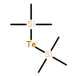
Co-reporter:Li Zheng, Xinhong Cheng, Duo Cao, Qian Wang, Zhongjian Wang, Chao Xia, Lingyan Shen, Yuehui Yu and Dashen Shen
RSC Advances 2015 vol. 5(Issue 50) pp:40007-40011
Publication Date(Web):27 Apr 2015
DOI:10.1039/C5RA04698J
The direct growth of Sb2Te3 on graphene is achieved by atomic layer deposition (ALD) with pre-(Me3Si)2Te treatment. The results of atomic force microscopy (AFM) indicate Volmer–Weber island growth is the dominant growth mode for ALD Sb2Te3 growth on graphene. High resolution transmission electron microscopy (HRTEM) analysis reveals perfect crystal structures of Sb2Te3 on graphene and no interface layer generation. The characterization of X-ray photoelectron spectroscopy (XPS) implies the impermeability of graphene can maintain Sb2Te3 intact and isolate the adverse effects of substrates. Our study provides a step forward to grow high quality Sb2Te3 at low temperature and expand the potential applications of graphene in ALD techniques.
Co-reporter:Duo Cao, Xinhong Cheng, Ya-Hong Xie, Li Zheng, Zhongjian Wang, Xinke Yu, Jia Wang, Dashen Shen and Yuehui Yu
RSC Advances 2015 vol. 5(Issue 47) pp:37881-37886
Publication Date(Web):21 Apr 2015
DOI:10.1039/C5RA04728E
Aluminum nitride (AlN) films have been deposited on AlGaN/GaN heterostructure substrates by plasma enhanced atomic layer deposition (PEALD). Different annealing treatments were adopted to change film structure and improve performance. Chemical composition, crystallinity, and electrical properties were studied for AlN films. The results show that some crystal grains appear in the films after annealing at a temperature of over 800 °C. The film crystalline quality increases as the annealing temperature rises. The N–O–Al bond decomposes during the high temperature annealing in N2, and some new N–Al bonds are formed in the AlN films. Annealing promotes the elemental interdiffusion between the films and the substrates. High-temperature annealing at 1000 °C in a nitrogen atmosphere can effectively promote complete nitridation of the AlN film, reduce the nitrogen vacancies, and cause the AlN film to form a semiconductor-like structure.
Co-reporter:Qian Wang, Xinhong Cheng, Zhongjian Wang, Chao Xia, Lingyan Shen, Li Zheng, Duo Cao, Yuehui Yu, DaShen Shen
Superlattices and Microstructures 2015 Volume 79() pp:1-8
Publication Date(Web):March 2015
DOI:10.1016/j.spmi.2014.11.026
•Partial silicon-on-insulator extended drain MOSFET is proposed.•Two new electric field peaks are introduced by the double step BOX layer.•The electric field in the BOX layer is enhanced by the buried N-type layer.•The proposed structure improves the breakdown voltage.•Self-heating effect is suppressed in the proposed structure.In this paper, a high voltage partial silicon-on-insulator (PSOI) extended drain metal–oxide–semiconductor (EDMOS) field effect transistor with a buried N-type layer (BNL) on the double-step buried oxide (DSBOX) is proposed. Due to the DSBOX, two additional peaks of the electric field are introduced in the drift region, modulating the electric field, achieving a more uniform distribution in the drift, and improving the lateral breakdown voltage (BV). The BNL provides a great population of positive charges on top of the DSBOX and enhances the electric field in the BOX, leading to a higher vertical BV. Moreover, the silicon window provides a thermal conduction path from the active region to the substrate, significantly alleviating the self-heating effect (SHE) in comparison to the conventional SOI-EDMOS (C-SOI).
Co-reporter:Li Zheng
The Journal of Physical Chemistry C 2015 Volume 119(Issue 11) pp:5995-6000
Publication Date(Web):March 5, 2015
DOI:10.1021/jp511562t
Co-reporter:Li Zheng, Xinhong Cheng, Duo Cao, Gang Wang, Zhongjian Wang, Dawei Xu, Chao Xia, Lingyan Shen, Yuehui Yu, and Dashen Shen
ACS Applied Materials & Interfaces 2014 Volume 6(Issue 10) pp:7014
Publication Date(Web):May 2, 2014
DOI:10.1021/am501690g
We improve the surface of graphene by atomic layer deposition (ALD) without the assistance of a transition layer or surface functionalization. By controlling gas–solid physical adsorption between water molecules and graphene through the optimization of pre-H2O treatment and two-step temperature growth, we directly grew uniform and compact Al2O3 films onto graphene by ALD. Al2O3 films, deposited with 4-cycle pre-H2O treatment and 100–200 °C two-step growing process, presented a relative permittivity of 7.2 and a breakdown critical electrical field of 9 MV/cm. Moreover, the deposition of Al2O3 did not introduce any detective defects or disorders in graphene.Keywords: Al2O3 films; gas−solid absorption; graphene; pre-H2O treatment;
Co-reporter:Li Zheng, Xinhong Cheng, Duo Cao, Dongliang Zhang, Zhongjian Wang, Dawei Xu, Chao Xia, Lingyan Shen and Yuehui Yu
RSC Advances 2014 vol. 4(Issue 83) pp:44296-44301
Publication Date(Web):12 Sep 2014
DOI:10.1039/C4RA07144A
We demonstrate the direct Al2O3–Gd2O3 double-films growth on graphene by H2O-assisted atomic layer deposition (ALD) using a hexamethyl disilazane precursor {Gd[N(SiMe3)2]3}. No defects are brought into graphene as shown by Raman spectra; the surface root-mean-square (RMS) roughness of the Al2O3–Gd2O3 double-films is down to 0.8 nm, comparable with the morphology of pristine graphene; the films are compact and continuous, and the relative permittivity is around 11, which indicate that H2O-assisted ALD can prepare high quality dielectric films on graphene.
Co-reporter:Duo Cao, Xinhong Cheng, Yahong Xie, Xiaolong Li, Zhongjian Wang, Chao Xia, Li Zheng, Dawei Xu, Lingyan Shen and Yuehui Yu
RSC Advances 2014 vol. 4(Issue 69) pp:36828-36833
Publication Date(Web):12 Aug 2014
DOI:10.1039/C4RA06542E
HfO2/La2O3 nanolaminate (HLOL) films were grown on AlGaN/GaN heterostructure by plasma enhanced atomic layer deposition (PEALD). After high-temperature rapid thermal annealing (RTA), the properties of the films were characterized. Si (coming from the La2O3 metal precursor) and La atoms diffuse into the HfO2 layer, cubic and tetragonal phase HfO2 exist in the HLOL film. The HLOL film has an effective dielectric constant of 35.7 and a breakdown electric field of 5.5 MV cm−1. Moreover, the HLOL film is an effective barrier to suppress the gate leakage current, which is 5 orders of magnitude lower compared to a conventional Schottky diode. The HLOL dielectric film on AlGaN/GaN could also improve the gate voltage swing range.
Co-reporter:Li Zheng, Xinhong Cheng, Duo Cao, Zhongjian Wang, Dawei Xu, Chao Xia, Lingyan Shen, Yuehui Yu
Materials Letters 2014 Volume 137() pp:200-202
Publication Date(Web):15 December 2014
DOI:10.1016/j.matlet.2014.08.146
•The effects of post-RTA at 800 °C for 30 s on elemental constituents, crystal structure and optical properties of HfAlO on graphene were explored.•After post-RTA, the hydroxyl groups were significantly reduced while HfAlO maintained amorphous due to Al-oxide permeation.•No additional defects were introduced into graphene, and no observable change of HfAlO morphology was detected after post-RTA.•The growing process of HfAlO on graphene by H2O-based ALD is compatible with the fabrication of graphene-based field effect transistors.In this work, we investigated the effects of post rapid thermal annealing (RTA) at 800 °C on structure and optical properties of HfAlO films directly grown on graphene by atomic layer deposition (ALD). Raman spectra indicated that no defects were introduced into graphene through film growth and RTA process. X-ray photoelectric (XPS) spectra showed that RTA contributed to thermal decomposition of hydroxides. Transmission electron microscopy (TEM) images and grazing incidence X-ray diffraction (GIXRD) patterns indicated that the amorphous morphology stability of HfAlO during the RTA process, and spectroscopic ellipsometry (SE) showed that RTA had few effects on optical properties of HfAlO on graphene.
Co-reporter:Chao Xia, Xinhong Cheng, Zhongjian Wang, Duo Cao, Tingting Jia, Li Zheng, Yuehui Yu, Dashen Shen
Microelectronics Reliability 2014 Volume 54(Issue 3) pp:582-586
Publication Date(Web):March 2014
DOI:10.1016/j.microrel.2013.10.021
•New P-SOI LDMOS structure with n-type floating buried layer in the substrate.•The proposed structure improves the BV and reduces specific on-resistance.•Self-heating effects are also suppressed in the proposed structure.In this paper, a novel high voltage lateral double diffused metal–oxide–semiconductor (LDMOS) field effect transistor based on partial silicon-on-insulator (PSOI) technology is proposed and investigated based on the numerical simulations. The structure is characterized by an n-type floating buried layer (NFBL) in the substrate under the silicon window near the drain. The buried layer in the substrate modulates the lateral and vertical electric field, which results in the electric field of the drift region distributed uniformly. Therefore, the breakdown voltage (BV) of the device is significantly improved. The influences of the key parameters on device performance of the proposed structure are discussed. Moreover, the self-heating effect (SHE) is greatly alleviated duo to the silicon window helps thermal conduction to the substrate, which improved the reliability of device application.
Co-reporter:T.T. Jia, X.H. Cheng, D. Chao, D.W. Xu, Z.J. Wang, C. Xia, Y.W. Zhang, Y.H. Yu
Nuclear Instruments and Methods in Physics Research Section B: Beam Interactions with Materials and Atoms 2013 Volume 307() pp:349-352
Publication Date(Web):15 July 2013
DOI:10.1016/j.nimb.2013.01.079
•LaAlO3 film was grown on GaAs by PEALD.•The LaAlO3 film remain amorphous after 500 °C annealing.•The GaAs/LaAlO3 interface was optimized by in situ NH3 plasma nitridation.•In situ NH3 plasma nitridation improved electric properties of MOS.In this work, we deposited LaAlO3 film on n-type GaAs by plasma enhanced atomic layer deposition (PEALD). In situ NH3 plasma nitridation of the GaAs surface was introduced to control the interface prior to plasma enhanced atomic layer deposition of LaAlO3. The chemical bonding state of NH3 plasma treated GaAs surface were investigated by X-ray photoelectron spectroscopy (XPS), which indicate that NH3 plasma nitridation can suppress interfacial growth on GaAs substrate. Transmission electron microscopy (TEM) images show the interface between LaAlO3 and GaAs was smooth and there was not obvious interface layer observed. The capacitance–voltage (C–V) and leakage current density–voltage (J–V) measurement indicate that the NH3 plasma nitridation improved the electrical properties of LaAlO3 films on GaAs substrate.
Co-reporter:Qian Wang, Xinhong Cheng, Li Zheng, Peiyi Ye, Menglu Li, Lingyan Shen, Jingjie Li, Dongliang Zhang, Ziyue Gu, Yuehui Yu
Applied Surface Science (1 July 2017) Volume 409() pp:
Publication Date(Web):1 July 2017
DOI:10.1016/j.apsusc.2017.02.257
•Composite TiAlO rather than TiO2-Al2O3 laminations is deposited on 4H-SiC by PEALD.•An interfacial layer composed of Ti, Si, O and C forms between TiAlO and 4H-SiC.•TiAlO offers competitive barrier heights (>1 eV) for both electrons and holes.Intermixing of TiO2 with Al2O3 to form TiAlO films on 4H-SiC is expected to simultaneously boost the dielectric constant and achieve sufficient conduction/valence band offsets (CBO/VBO) between dielectrics and 4H-SiC. In this work, a composite TiAlO film rather than TiO2-Al2O3 laminations is deposited on 4H-SiC by plasma enhanced atomic layer deposition (PEALD). X-ray photoelectron spectroscopy (XPS) is performed to systematically analyze the interfacial chemistry and energy band alignment between TiAlO and 4H-SiC. An interfacial layer composed of Ti, Si, O and C forms between TiAlO and 4H-SiC during PEALD process. The VBO and CBO between TiAlO and 4H-SiC are determined to be 1.45 eV and 1.10 eV, respectively, which offer competitive barrier heights (>1 eV) for both electrons and holes and make it suitable for the fabrication of 4H-SiC metal-oxide-semiconductor field effect transistors (MOSFETs).
Co-reporter:Li Zheng, Xinhong Cheng, Yuehui Yu, Yahong Xie, Xiaolong Li and Zhongjian Wang
Physical Chemistry Chemical Physics 2015 - vol. 17(Issue 5) pp:NaN3185-3185
Publication Date(Web):2014/12/11
DOI:10.1039/C4CP04957H
Graphene has been drawing worldwide attention since its discovery in 2004. In order to realize graphene-based devices, thin, uniform-coverage and pinhole-free dielectric films with high permittivity on top of graphene are required. Here we report the direct growth of Al2O3-doped HfO2 films onto graphene by H2O-based atom layer deposition (ALD). Al2O3-onto-HfO2 stacks benefited the doping of Al2O3 into HfO2 matrices more than HfO2-onto-Al2O3 stacks did due to the micro-molecular property of Al2O3 and the high chemical activity of trimethylaluminum (TMA). Al2O3 acted as a network modifier, maintained the amorphous structure of the film even to 800 °C, and made the film smooth with a root mean square (RMS) roughness of 0.8 nm, comparable to the surface of pristine graphene. The capacitance and the relative permittivity of Al2O3-onto-HfO2 stacks were up to 1.18 μF cm−2 and 12, respectively, indicating the high quality of Al2O3-doped HfO2 films on graphene. Moreover, the growth process of Al2O3-doped HfO2 films introduced no detective defects into graphene confirmed by Raman measurements.