Co-reporter:Ryo Kawajiri, Hideyuki Takagishi, Takashi Masuda, Toshihiko Kaneda, Ken Yamazaki, Yasuo Matsuki, Tadaoki Mitani and Tatsuya Shimoda
Journal of Materials Chemistry A 2016 vol. 4(Issue 16) pp:3385-3395
Publication Date(Web):05 Feb 2016
DOI:10.1039/C5TC03684D
Well-defined silicon patterns with a high aspect ratio and sharp edges were directly formed by imprinting of liquid silicon which was synthesized via the photopolymerization of cyclopentasilane (CPS: Si5H10) with UV light. After the patterns were formed, they were converted into amorphous silicon patterns by post-annealing at 400 °C. Both dotted and lined patterns whose size ranges from 1 μm to 100 nm were obtained, suggesting that their size could be further reduced. It is very noteworthy that all the obtained patterns demonstrated a good aspect ratio and sharp edges, despite a large shrinkage of 70–80% during the process. By conducting solid-phase crystallization at 800 °C, the pattern portion was converted into polycrystalline pure silicon, whereas the residual film region remained in an amorphous state containing large amounts of oxygen and carbon atoms. Based on the experimental results, the relationship between the decomposition and solidification processes of liquid silicon and its imprinting behavior was clarified and the mechanism of impurity condensation in a residual film region at the annealing temperature of 800 °C and that of well-defined shape formation were discussed. The developed method can be expected to be used in the fabrication of micro-silicon devices because of its production simplicity.
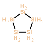
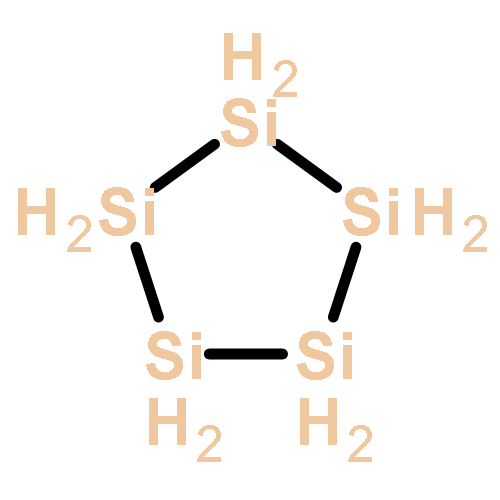
Co-reporter:Zhongrong Shen, Takashi Masuda, Hideyuki Takagishi, Keisuke Ohdaira and Tatsuya Shimoda
Chemical Communications 2015 vol. 51(Issue 21) pp:4417-4420
Publication Date(Web):09 Feb 2015
DOI:10.1039/C4CC09026H
Cyclopentasilane converts into amorphous silicon film between two parallel substrates under atmospheric pressure by thermal decomposition at 350–400 °C, which combines the advantages of high throughput with cost reduction and high quality film formation.
Co-reporter:Toshihiko Kaneda, Daisuke Hirose, Takaaki Miyasako, Phan Trong Tue, Yoshitaka Murakami, Shinji Kohara, Jinwang Li, Tadaoki Mitani, Eisuke Tokumitsu and Tatsuya Shimoda
Journal of Materials Chemistry A 2014 vol. 2(Issue 1) pp:40-49
Publication Date(Web):01 Nov 2013
DOI:10.1039/C3TC31842G
Technologies of device printing have been widely explored, but existing printing techniques still cannot produce well-defined patterns required by fine electronic devices. Here, a new printing method is proposed and the printing of metal-oxide patterns with well-defined shapes was demonstrated. Excellent thin-film transistors with channel lengths around 500 nm were completely printed by this method in an air atmosphere. This printing utilizes a viscoelastic transformation of the precursor gel when imprinted; it softens at a certain temperature during thermal-imprinting so that the gel can be rheologically imprinted. The imprinted pattern shows very small shrinkage during post-annealing, thereby achieving a high shape fidelity to the mould; this results from metal-oxide condensation at imprinting. The viscoelastic transformation and metal-oxide condensation at imprinting constitute the basis for this printing method, which is closely related to the cluster structure in the precursor gel. This method has worked for patterns down to several tens of nanometers.
Co-reporter:Zhongrong Shen ; Yasuo Matsuki
Journal of the American Chemical Society 2012 Volume 134(Issue 19) pp:8034-8037
Publication Date(Web):April 30, 2012
DOI:10.1021/ja301956s
For generation of a fine aluminum pattern by conventional vacuum processing, it is necessary not only to use complex and costly instruments but also to perform an additional etching process, which may result in physical and chemical damage to the target film surface. Herein we report a simple solution process for the selected deposition of an Al pattern. Al is obtained from the decomposition of alane under dehydrogenation catalysis of a Pt nanocrystalline pattern on a substrate at ∼105–120 °C, while the self-decomposition of alane in solution is avoided in the presence of high-boiling-point amine. This deposited film generates Al crystals with a diameter of several hundred nanometers, following an epitaxial growth to a continual film. The obtained film shows high conductivity, with a resistivity close to that of bulk Al.
Co-reporter:Zhongrong Shen, Jinwang Li, Yasuo Matsuki and Tatsuya Shimoda
Chemical Communications 2011 vol. 47(Issue 36) pp:9992-9994
Publication Date(Web):31 May 2011
DOI:10.1039/C1CC12138C
In contrast to the traditional chemical vapor deposition technique under high vacuum, we introduce a deposition method in liquid to prepare Pt patterns on substrate near 100 °C by seed growth.
Co-reporter:Zhongrong Shen, Yasuo Matsuki and Tatsuya Shimoda
Chemical Communications 2010 vol. 46(Issue 45) pp:8606-8608
Publication Date(Web):04 Oct 2010
DOI:10.1039/C0CC02829K
We describe the synthesis of single-crystalline Pt nanocubes with a large diameter (around 35 nm) using a solvent-thermal reaction in a polarity-controlled mixture of 1-butanol, toluene, and N,N-dimethylformamide at 185 °C.
Co-reporter:Zhongrong Shen, Takashi Masuda, Hideyuki Takagishi, Keisuke Ohdaira and Tatsuya Shimoda
Chemical Communications 2015 - vol. 51(Issue 21) pp:NaN4420-4420
Publication Date(Web):2015/02/09
DOI:10.1039/C4CC09026H
Cyclopentasilane converts into amorphous silicon film between two parallel substrates under atmospheric pressure by thermal decomposition at 350–400 °C, which combines the advantages of high throughput with cost reduction and high quality film formation.
Co-reporter:Zhongrong Shen, Jinwang Li, Yasuo Matsuki and Tatsuya Shimoda
Chemical Communications 2011 - vol. 47(Issue 36) pp:NaN9994-9994
Publication Date(Web):2011/05/31
DOI:10.1039/C1CC12138C
In contrast to the traditional chemical vapor deposition technique under high vacuum, we introduce a deposition method in liquid to prepare Pt patterns on substrate near 100 °C by seed growth.
Co-reporter:Zhongrong Shen, Yasuo Matsuki and Tatsuya Shimoda
Chemical Communications 2010 - vol. 46(Issue 45) pp:NaN8608-8608
Publication Date(Web):2010/10/04
DOI:10.1039/C0CC02829K
We describe the synthesis of single-crystalline Pt nanocubes with a large diameter (around 35 nm) using a solvent-thermal reaction in a polarity-controlled mixture of 1-butanol, toluene, and N,N-dimethylformamide at 185 °C.
Co-reporter:Ryo Kawajiri, Hideyuki Takagishi, Takashi Masuda, Toshihiko Kaneda, Ken Yamazaki, Yasuo Matsuki, Tadaoki Mitani and Tatsuya Shimoda
Journal of Materials Chemistry A 2016 - vol. 4(Issue 16) pp:NaN3395-3395
Publication Date(Web):2016/02/05
DOI:10.1039/C5TC03684D
Well-defined silicon patterns with a high aspect ratio and sharp edges were directly formed by imprinting of liquid silicon which was synthesized via the photopolymerization of cyclopentasilane (CPS: Si5H10) with UV light. After the patterns were formed, they were converted into amorphous silicon patterns by post-annealing at 400 °C. Both dotted and lined patterns whose size ranges from 1 μm to 100 nm were obtained, suggesting that their size could be further reduced. It is very noteworthy that all the obtained patterns demonstrated a good aspect ratio and sharp edges, despite a large shrinkage of 70–80% during the process. By conducting solid-phase crystallization at 800 °C, the pattern portion was converted into polycrystalline pure silicon, whereas the residual film region remained in an amorphous state containing large amounts of oxygen and carbon atoms. Based on the experimental results, the relationship between the decomposition and solidification processes of liquid silicon and its imprinting behavior was clarified and the mechanism of impurity condensation in a residual film region at the annealing temperature of 800 °C and that of well-defined shape formation were discussed. The developed method can be expected to be used in the fabrication of micro-silicon devices because of its production simplicity.
Co-reporter:Toshihiko Kaneda, Daisuke Hirose, Takaaki Miyasako, Phan Trong Tue, Yoshitaka Murakami, Shinji Kohara, Jinwang Li, Tadaoki Mitani, Eisuke Tokumitsu and Tatsuya Shimoda
Journal of Materials Chemistry A 2014 - vol. 2(Issue 1) pp:NaN49-49
Publication Date(Web):2013/11/01
DOI:10.1039/C3TC31842G
Technologies of device printing have been widely explored, but existing printing techniques still cannot produce well-defined patterns required by fine electronic devices. Here, a new printing method is proposed and the printing of metal-oxide patterns with well-defined shapes was demonstrated. Excellent thin-film transistors with channel lengths around 500 nm were completely printed by this method in an air atmosphere. This printing utilizes a viscoelastic transformation of the precursor gel when imprinted; it softens at a certain temperature during thermal-imprinting so that the gel can be rheologically imprinted. The imprinted pattern shows very small shrinkage during post-annealing, thereby achieving a high shape fidelity to the mould; this results from metal-oxide condensation at imprinting. The viscoelastic transformation and metal-oxide condensation at imprinting constitute the basis for this printing method, which is closely related to the cluster structure in the precursor gel. This method has worked for patterns down to several tens of nanometers.
![Poly[(5,7-dihydro-1,3,5,7-tetraoxobenzo[1,2-c:4,5-c']dipyrrole-2,6(1H,3H)-diyl)-1,4-phenyleneoxy-1,4-phenylene]](http://img.cochemist.com/ccimg/25100/25036-53-7.png)
![Poly[(5,7-dihydro-1,3,5,7-tetraoxobenzo[1,2-c:4,5-c']dipyrrole-2,6(1H,3H)-diyl)-1,4-phenyleneoxy-1,4-phenylene]](http://img.cochemist.com/ccimg/25100/25036-53-7_b.png)